DESCRIPTION
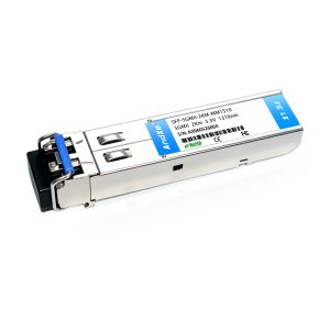
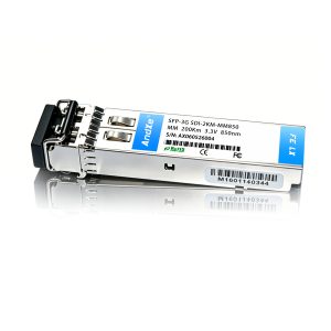
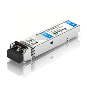
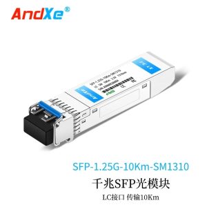
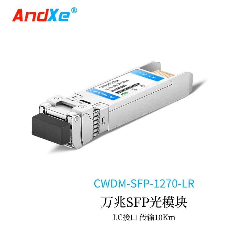
This CWDM DFB 10Gigabit SFP+ transceiver is designed to transmit and receive optical data over single mode optical fiber for link length 10km.
The SFP+ LR module electrical interface is compliant to SFI electrical specifications. The transmitter input and receiver output impedance is 100 Ohms differential. Data lines are internally AC coupled. The module provides differential termination and reduce differential to common mode conversion for quality signal termination and low EMI. SFI typically operates over 200 mm of improved FR4 material or up to about 150mmof standard FR4 with one connector.
The transmitter converts 10Gbit/s serial CML electrical data into serial optical data compliant with the 10GBASELR standard. An open collector compatible Transmit Disable (TxDis) is provided. A logic “1,” or no connection on this pin will disable the laser from transmitting. A logic “0” on this pin provides normal operation. The transmitter has an internal automatic power control loop (APC) to ensure constant optical power output across supply voltage and temperature variations. An open collector compatible Transmit Fault (TFault) is provided. TXFault is a module output contact that when high, indicates that the module transmitter has detected a fault condition related to laser operation or safety. The TXFault output contact is an open drain/collector and shall be pulled up to the VccHost in the host with a resistor in the range 4.7-10 kΩ . TXDisable is a module input contact. When TXDisable is asserted high or left open, the SFP+ module transmitter output shall be turned off. This contact shall be pulled up to VccT with a 4.7 kΩ to 10 kΩ resistor
The receiver converts 10Gbit/s serial optical data into serial PECL/CML electrical data.An open collector compatible Loss of Signal is provided. RxLOS when high indicates an optical signal level below that specified in the relevant standard. The RxLOS contact is an open drain/collector output and shall be pulled up to VccHost in the host with a resistor in the range 4.7-10 kΩ, or with an active termination. Power supply filtering is recommended for both the transmitter and receiver. The RxLOS signal is intended as a preliminary indication to the system in which the SFP+ is installed that the received signal strength is below the specified range. Such an indication typically points to non-installed cables, broken cables, or a disabled, failing or a powered off transmitter at the far end of the cable.
Features
● 10Gb/s serial optical interface compliant to 802.3ae 10GBASE-LR
● Electrical interface compliant to SFF-8431 specifications for enhanced 8.5 and 10 Gigabit small form factor pluggable module “SFP+”
● CWDM DFB transmitter, PIN photo-detector
● 2-wire interface for management specifications compliant with SFF 8472 digital diagnostic monitoring interface for optical transceivers
● Operating case temperature: 0 to 70 °C or-40 to 85 °C
● ll-metal housing for superior EMI performance
● Low power consumption
● Advanced firmware allow customer system encryption information to be stored in transceiver
● Cost effective SFP+ solution, enables higher port densities and greater bandwidth
● RoHS compliant
Applications
● High-speed storage area networks
● Computer cluster cross-connect
● Custom high-speed data pipes
ABSOLUTE MAXIMUM RATING
These values represent the damage threshold of the module. Stress in excess of any of the individual Absolute Maximum Ratings can cause immediate catastrophic damage to the module even if all other parameters are within Recommended Operating Conditions.
| Parameters | Symbol | Min. | Max. | Unit |
| Power Supply Voltage | VCC | 0 | 3.6 | V |
| Storage Temperature | Tc | -40 | 85 | 。C |
| Operating Case Temperature | Tc | 0 | 70 | 。C |
| TI | -40 | 85 | ||
| Relative Humidity | RH | 5 | 95 | % |
| RX Input Average Power | Pmax | – | 0 | dBm |
Table 1: Absolute Maximum Rating
RECOMMENDED OPERATING ENVIRONMENT
Recommended Operating Environment specifies parameters for which the electrical and optical characteristics hold unless otherwise noted.
| Parameters | Symbol | Min. | Typical | Max | Unit |
| Power Supply Voltage | VCC | 3.135 | 3.3 | 3.465 | V |
| Power Supply Current | Icc | 350 | mA | ||
| Operating Case Temperature | TC | 0 | 25 | 70 | 。C |
| TI | -40 | 25 | 85 |
Table 2: Recommended Operating Environment
7. OPTICAL CHARACTERISTICS
The following optical characteristics are defined over the Recommended Operating Environment unless otherwise specified.
| Parameters | Unit | Values |
| Operating Reach | m | 10K |
| Transmitter | ||
| Center wavelength (range) | nm | λ+ -6.5 |
| Side Mode Suppression Ratio (min) | dB | 30 |
| Launched power | ||
| – maximum (Average) | dBm | +6 |
| – minimum (Average) | dBm | 1 |
| Transmitter and dispersion penalty (max) | dB | 3.2 |
| Average launch power of OFF transmitter (max) | dBm | -30 |
| Extinction ratio (min) | dB | 3.5 |
| RIN12 OMA (max) | dB/Hz | -128 |
| Optical Return Loss Tolerance (min) | dB | 12 |
| Receiver | ||
| Center wavelength (range) | nm | 1260-1620 |
| Receive overload (max) in average power(note 1) | dBm | 0.5 |
| Receive sensitivity (min) in average power(note 1) | dBm | -14.4 |
| Receiver Reflectance (max) | dB | -12 |
| Los Assert(min) | dBm | -30 |
| Los Dessert(max) | dBm | -16 |
| Los Hysteresis(min) | dB | 0.5 |
| Receive electrical 3dB upper cutoff frequency (max) | GHz | 12.3 |
| Receiver power (damage, Max) | dBm | +7 |
Table 3: Optical Characteristics
Notes:
1. Average optical power shall be measured using the methods specified in TIA/EIA-455-95.
2. Power budget is defined as the different between the Rx sensitivity and the Tx output power of the interface.
3. Path penalty is intended as the power penalty of the interface between back-to-back and the maximum applied dispersion.
ELECTRICAL CHARACTERISTICS
The following electrical characteristics are defined over the Recommended Operating Environment unless otherwise specified.
| Parameter | Symbol | Min. | Typical | Max | Unit | Notes | ||||||||
| Data Rate | – | 10.3125 | – | Gbps | ||||||||||
| Power Consumption | – | 800 | 1000 | mW | ||||||||||
| Transmitter | ||||||||||||||
| Single Ended Output Voltage Tolerance | -0.3 | – | 4 | V | ||||||||||
| C common mode voltage tolerance | 15 | – | – | mV | ||||||||||
| Tx Input Diff Voltage | VI | 180 | 800 | mV | ||||||||||
| Tx Fault | VoL | -0.3 | 0.4 | V | At 0.7mA | |||||||||
| Data Dependent Input Jitter | DDJ | 0.1 | UI | |||||||||||
| Data Input Total Jitter | TJ | 0.28 | UI | |||||||||||
| Receiver | ||||||||||||||
| Single Ended Output Voltage Tolerance | -0.3 | – | 4 | V | ||||||||||
| Rx Output Diff Voltage | Vo | 300 | 850 | mV | ||||||||||
| Rx Output Rise and Fall Time | Tr/Tf | 30 | ps | 20% to 80% | ||||||||||
| Total Jitter | TJ | 0.7 | UI | |||||||||||
| Deterministic Jitter | DJ | 0.42 | UI | |||||||||||
Table 4: Electrical Characteristics
MECHANICAL
Comply to SFF-8432 rev. 5.0, the improved Pluggable form factor specification.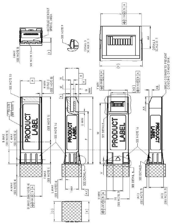
安科士 | AndXe Networks
企业邮箱:susie@andxe.com
企业手机:182 8033 7727
本产品仅展示部分参数,如有需要,请联系我们。
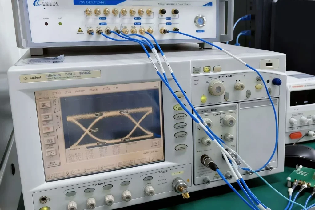
功率和波长测试
测试信号发射强度和波长,确保接收机的信号解码能力,以及从发射机到接收机的波长保持一致。
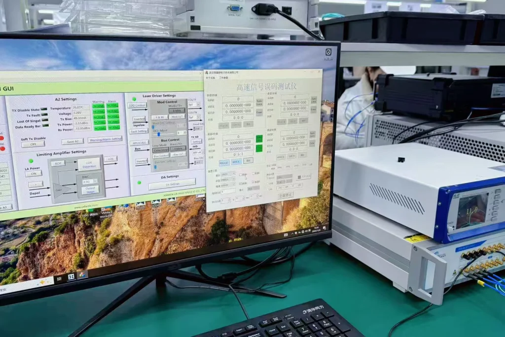
流量测试
测试误码率、丢包率,使其满足相应标准,保证收发器的性能。
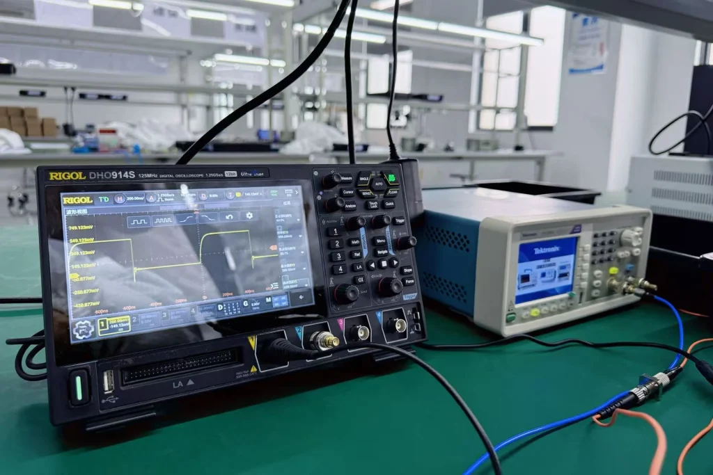
光学性能测试
测试收发器的眼图情况、接收灵敏度、消光比、波长、发光、收光、电流、电压等,确保信号传输的质量、稳定性和可靠性。
光学性能测试
测试收发器的眼图情况、接收灵敏度、消光比、波长、发光、收光、电流、电压等,确保信号传输的质量、稳定性和可靠性。
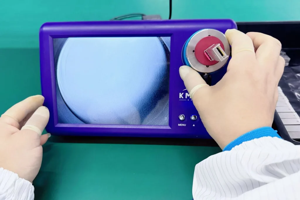

兼容品牌:
思科 | 瞻博网络 | Arista | Brocade | HPE ProCurve | HPE Aruba | HPE BladeSystem | HPE H3C | H3C | 戴尔 | Extreme | HW | Generic | F-tone | 英特尔Netgear | IBM | NVIDIA/Mellanox(以太网)| Ciena | Fortinet | Avago | Avaya | 阿尔卡特朗讯 | D-Link | F5 | Ubiquiti | Mikrotik | Broadcom…..